【APR】innovus流程
innovus流程
PART A. open MMMC Browser
🛠️STEP-A1. Library Set
library Set:  1. slow.lib
              2. xxx18io3v5v_slow.lib
🛠️STEP-A2. RC Corner
Name: RC_MAX
Cap Table : xxx18_1p6m.captbl [給trial Route時計算RC用的][算是查表的模型]
temperature : 125
QRC technologi File : RCGen.tch
🛠️STEP-A3. Delay Corners
Delay Corner = library Set ( 包含Timing(.lib) + SI(.cdb) ) + RC Corner
🛠️STEP-A4. Constrain Mode
🛠️STEP-A5. Create Analysis Views
不同的Delay Corner 和 不同的Constrain Mode
組合成不同的Aanlysis View
Name
Constraint Mode + Delay Corner
Example
Name:               CHECK_SETUP_TIME
Constraint Mode :   CHIP_SDC
Delay Corner:       DELAY_MAX
🛠️STEP-A6. In MMMC Browser - Setup/Hold Analysis Views
Setup the analysis views for setup time analysis.
上面設定好的 Analysis View 再來設定哪種要用來Setup Analysis,哪種要用來Hold Analysis
Example:
Setup Analysis Views : CHECK_SETUP_TIME(這是step5建立好的Analysis Views)
Hold Analysis Views  : CHECK_HOLD_TIME(一樣是step5建立好的Analysis Views)
STEP-A1. ~ STEP-A6. 都完成後可以看到下圖
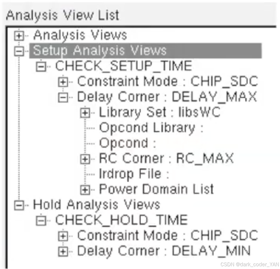
以上步驟設定完後可以透過save the MMMC view將以上設定存成CHIP_MMMC.view
下次開啟innovus用Design import 呼叫CHIP_MMMC.view就可以了
- ⚠️TODO 補CHIP_MMMC.view程式碼
Import Design
存成CHIP.globals
PART B. Floorplanning
Core Limited Design
- 決定因素:晶片面積由 Core(核心邏輯與記憶體) 的大小決定 。
- 情境:當內部邏輯電路非常複雜、佔用面積大,但外部需要的 I/O 腳位較少時。
- 特徵:Core 的邊長大於所有 IO Pad 排列所需的長度。為了維持 I/O Power Ring 的連接性,必須在 IO Pad 之間插入 Pad Filler 來填補空隙 。
Pad Limited Design
- 決定因素:晶片面積由 I/O Pad 的數量決定 。
- 情境:當內部邏輯很簡單(面積小),但外部需要連接大量訊號(I/O 腳位多)時,比如說test chip 。
- 特徵:為了排下所有的 IO Pad,晶片邊長被迫拉大,導致 Core 內部會有大量的閒置空間(Utilization 低),這在成本上較不划算,因為你為不需要的矽面積付了錢 。
core utilization:
Core Utilization(核心利用率) 是指在晶片核心區域(Core Area)中,標準單元(Standard Cells)實際佔用面積的百分比 。
Floorplanning in Innovus
🛠️STEP-B1. Setup the floorplan
Define core width, height and core margin
- For pad limited design
• SetCore to IO Boundaryto a suitable value, such as 100 (design dependent)
• Then, setDie Size Width and Heightto suitable value
• ClickApply - For core limited design
• SetCore to IO Boundaryto a suitable value
• SetCore WidthandHeightto the demanded value
• ClickApply
Macro blocks require manual placement
PART C. Power Planning
Power Issue: IR Drop ⭐️⭐️⭐️
IR Drop (電壓降) 是指電流流經電源與接地網路的電阻時,產生的電壓損耗 ( V = I × R ) (V=I×R) (V=I×R)
- IR drop can cause the chip to fail due to
• Performance (circuit running slower than specificatio))
• Functionality problem (setup or hold violations)
• Unreliabie operation (less noise margin)
• Power consumption (leakage power)
• Latch up
Power Issue: Electromigration
Electromigration (電遷移) 是指金屬導線在長時間高電流密度運作下產生的一種「老化」或磨損機制
發生在current density較高的地方
Experience: make current density of power ring < 1mA/um
要知道流過的電流多大,來計算線寬,來降低current density
避免Electromigration的問題太快的發生
– Calculating power/ground ring width –
- slot rule
- Calculate stripe set
- 主要目的: 透過增加電源線的密度來縮短電流路徑,有效降低電阻,防止 IR Drop(電壓降) 導致晶片效能下降或功能失效
- 這可以用基本的物理公式 R = ρ × W / L R=ρ× W/L R=ρ×W/L (電阻 = 電阻率 × 長度 / 寬度)來解釋:
-
- 縮短長度 ( L L L): 在晶片中,電流必須從 Power Ring 或 Stripe 流經細小的金屬線才能到達標準單元。增加 Stripe (電源條) 的密度,就像在城市中增加更多主幹道,讓單元能以更短的距離 ( L L L 變小) 連接到主電源網 。
-
- 降低電阻( R R R): 根據公式,導線長度 ( L L L) 變短,路徑上的總電阻 ( R R R) 就會直接下降。
-
- 減少電壓降 ( V = I R V=IR V=IR): 電阻降低後,根據歐姆定律,IR Drop (電壓降) 自然也會隨之減少,確保晶片獲得足夠的工作電壓。
- Core/IO power pad selection
- Core power pad
- IO power pad
Power Planning - by Experience
– Calculating power/ground ring width –
– slot rule –
– Calculate stripe set –
– Core/IO power pad selection –
Power Planning - Global Net Connection
Power Planning in Innovus
– Create power rings and power stripes –
– Create power ring –
Power Planning - Ring
Power Planning - Stripe
– Create power stripes –
– Spacing and Set Pattern Definitions –
Power Planning - Special Route
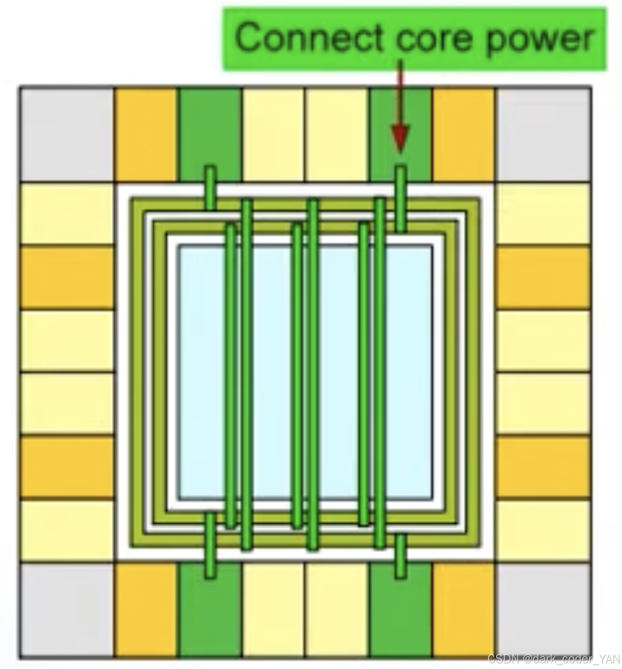
Use Special Route to connect the core power pins
Route > Special Route...
- Pad Pins (Connect core power Pins)
把Pad上的VDD和GND接到Power Network上的Ring跟stripes
PART D. Pre-CTS Optimization
– Pre-CTS timing analysis –
下指令timeDesign -preCTS,這是在 clk network 是 ideal(no clock skew)的狀況下進行的分析。
這裡最有可能出問題的是 global reset,因為它需要連接多個模塊。
在 synthesis 階段,reset 是 ideal 的,但現在包含了 wire 的寄生參數,導致 global reset 的 loading 很大。
global reset 的 loading 過大會導致 transition time 變差,從而引發 setup/hold violation。
– Pre-CTS timing analysis –
下指令timeDesign -preCTS
這是在 clk network是idea(no clock skew) 的狀況下
這邊最有可能出問題的就是global reset 因為他要接給很多人用
在synthesis階段,reset是idea的
但是現在包含了wire進去,這個global reset的Loading很大
WNS: Worst-case Negative Timing Slack (WNS)
TNS: Total Negative Timing Slack (TNS)
這兩個要修成正的
– Pre-CTS optimization –
– optDesign command –
- To optimize timing placed design for the first time with ideal clocks
optDesign -preCTS - To further optimize a design after above command execution
optDesign -preCTS -incr
PART E. Clock Tree Synthesis
– Hybrid Clock Mesh for reducing skew and power –
Clock Mesh Network降低OCV (on-chip variation)的問題
– Create clock tree specification file from the SDC constraints –
innovus> create_copt_clock_tree_spec -file CHIP.CCOPT.spec -keep_all_sdc_clocks
– Load Clock Tree Spec. and Synthesis Clock Tree –
innovus> source CHIP.CCOPT.spec
innovus> ccopt_design
– Routed H-tree clock network –
– Display Clock Tree –
可以看到最大的clock skew
PART F. Post-CTS Optimization
-
Post-CTS timing analysis
•Type the following command in the command line to check setup time
timeDesign -postCTS預設省略(-setup)
• Type the following command in the command line to check hold time
timeDesign -postCTS -hold
檢查.cap、.fanout、.tran -
Post-CTS Optimization
optDesign command
• To correct setup violations and design rule violation
optDesign -postCTS預設省略(-setup)
這邊有問題通常會是clk skew造成
• To correct hold violations
optDesign -postCTS -hold
補充:
if hold time 一直修不好
可能情況:
(1)
這邊會包含前面步驟設定的MMMC一併分析
練習
Q: 在進行APR之前,為何需要從合成工具(Design Compiler)產生的SDC檔案中移除 set_dont_touch_network 指令?
因為APR工具有內建的時脈樹綜合(CTS)引擎,必須要能自由處理時脈網路。
此指令會防止工具修改時脈(clk)和重置(reset)等高扇出網路,但在APR階段,CTS需要對這些網路進行緩衝器插入與繞線以滿足時序要求。
Q: 在規劃I/O Pad佈局時,對於Clock Pad的安排有何特殊考量以提升訊號完整性?
在其兩側使用VSS Pad將其夾住。
建議用VSS Pad將Clock Pad夾住,可以提供遮蔽效果,防止相鄰訊號線的雜訊耦合干擾時脈訊號的穩定性。
Q: 在MMMC(Multi-Mode Multi-Corner)設定檔中,create_delay_corner 指令的作用是什麼?
組合一個 timing_condition 和一個 rc_corner,形成一個完整的延遲計算情境。
根據MMMC的階層結構,create_delay_corner用於將代表元件延遲的timing_condition與代表繞線寄生參數的rc_corner 結合起來。

有“AI”的1024 = 2048,欢迎大家加入2048 AI社区
更多推荐

 25
25 0
0- 0


 已为社区贡献2条内容

所有评论(0)